


High purity metals and alloys such as aluminum, zinc, cobalt, copper, titanium, zirconium, molybdenum, magnesium, and stainless steel are the backbone of many industries, from electronics to aerospace, and medical devices.
Due to the critical nature of many of the components made from these materials, high purity alloys should be highly consistent, with extremely low levels of impurities and contaminations. This is driving non-destructive inspection using Scanning Acoustic Microscopy (SAM) to identify small inclusions and other defects as small as 50-microns.
Scanning Acoustic Microscopy (SAM) is widely accepted in the semiconductor industry as a failure analysis and reliability detection metrology technology. Now the same technology, with variations in instrumentation and adaption for different use cases, is being applied to high purity metals and alloys.
The challenge, however, is performing 100% inspection at sufficient throughput speeds to remove materials with defects that do not meet strict quality requirements. As with other inspection systems, increasing scanning speed traditionally meant sacrificing scanning image resolution.
Fortunately, recent advancements in SAM technology have significantly improved throughput speeds and defect detectability.
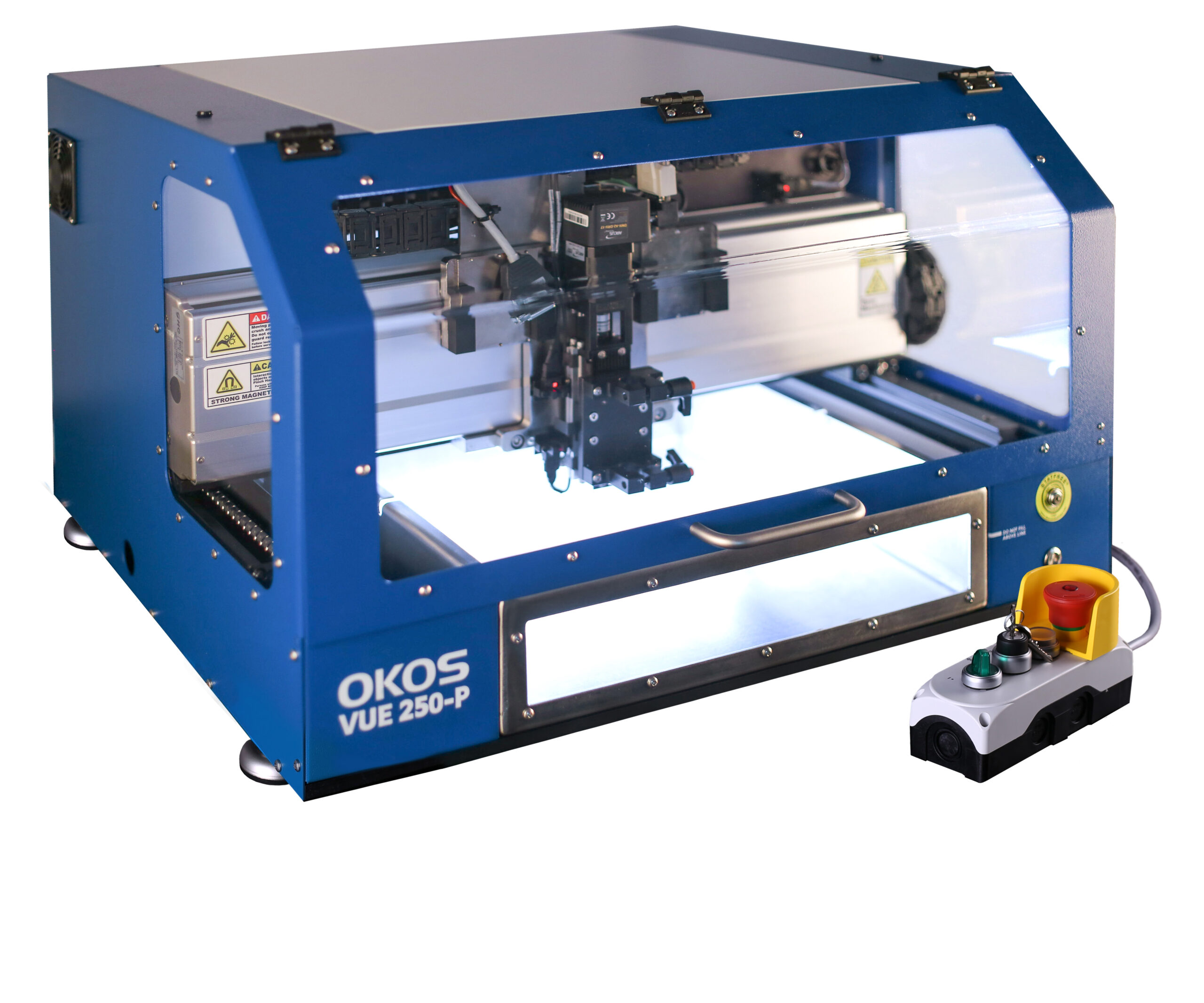 “While a conventional 5 MHz sensor could take up to 45 minutes to inspect an 8–10-inch square or disc alloy, an advanced phased array with 64-128 sensors and innovative software to render the images reduces inspection time to five minutes with more granular detection of small impurities or defects,” says Hari Polu, President of OKOS, a Virginia-based manufacturer of SAM and industrial ultrasonic non-destructive (NDT) systems. OKOS is a wholly-owned subsidiary of PVA TePla AG, Germany, and offers both manual and automated inspection systems for flat panels, thin plates, circular discs, sputtering targets, and special alloys.
By dramatically increasing inspection speed, Polu says the specialty metals industry is no longer limited to selective sample testing during In-Process Quality Control. Although SAM has long been utilized for this type of inspection, the testing involved a handheld unit or a multi-point inspection. Now it is more feasible to conduct a 100% inspection of the entire surface/interface.
In addition, these advances also facilitate the detection of not just gross defects, but much smaller defects, to drive highly consistent high yield products.
“Advanced, phased array SAM systems make it possible for specialty metals divisions to move to a higher level of failure analysis because of the level of detection and precision involved,” says Polu. “In the past, detecting a 500-micron defect was the goal; now it is a 50-micron defect. And with high purity metals, they want to inspect every item, not just a few samples.”
 Scanning Acoustic Microscopy
SAM is a non-invasive and non-destructive ultrasonic testing method. The testing is already the industry standard for 100% inspection of semiconductor components to identify defects such as voids, cracks, and the delamination of different layers within microelectronic devices. Now, the same rigor of failure analysis and quality testing is being applied to specialty metals and alloys to detect subsurface flaws, dis-bonds, cracks, and other irregularities.
Scanning acoustic microscopy works by directing focused sound from a transducer at a small point on a target object. The sound hitting the object is either scattered, absorbed, reflected, or transmitted. By detecting the direction of scattered pulses as well as the “time of flight,” the presence of a boundary or object can be determined as well as its distance.
To produce an image, samples are scanned point by point and line by line. Scanning modes range from single-layer views to tray scans and cross-sections. Multi-layer scans can include up to 50 independent layers. Depth-specific information can be extracted and applied to create two- and three-dimensional images without the need for time-consuming tomographic scan procedures and more costly X-rays. The images are then analyzed to detect and characterize flaws such as cracks, inclusions, and voids.
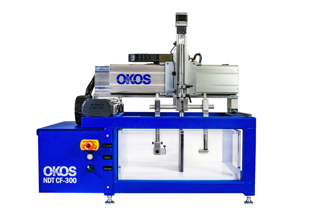
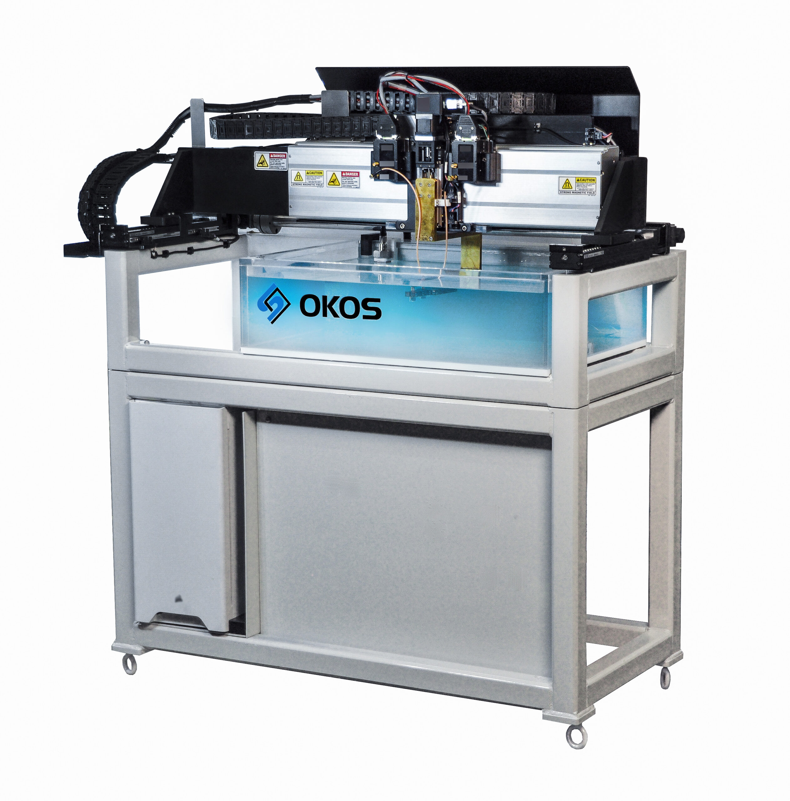
When high throughput is required for 100% inspection, ultra-fast single or dual gantry scanning systems are utilized along with 128 sensors for phased array scanning. Multiple transducers can also be used to simultaneously scan for higher throughput.
“In tests with a Fortune 500 multinational company on a sample of this aluminum and steel, the equipment was able to scan the material in three minutes. Before, it was taking them 40 minutes to do one part,” says Polu.
 OKOS Software
As important as the physical and mechanical aspects of conducting a scan, the software is critical to improving the resolution and analyzing the information to produce detailed scans.
Multi-axis scan options enable A, B, and C-scans, contour following, off-line analysis, and virtual rescanning for composites, metals, and alloys, which result in highly accurate internal and external inspection for defects and thickness measurement via the inspection software.
“OKOS decided early on to deliver a software-driven, ecosystem-based solution,” said Polu. The company’s ODIS Acoustic Microscopy software supports a wide range of transducer frequencies from 2.25 to 230 MHz.
Polu estimates that the company’s software-driven model enables them to drive down the costs of SAM testing while delivering the higher quality of inspection results at faster speeds.
“In the electronics, aerospace, medical device, and other industries, there is an increasing demand for inspection equipment that can perform non-destructive imaging and materials analysis,” says Polu. “With more sensors and advanced software to interpret the information at very high resolutions, specialty metals manufacturers can inspect 100% of the materials at a level one to two orders of magnitude better to discover flaws that were previously undetected.”


