In the early 90s, CAD/CAM seemed to be the “happening” technology in the design chain. 3D modeling of products and sharing of that data, enabled the Dfx mantra (design for manufacturing, design for assembly, design for service, design for quality, etc). Together with client-server computing this data sharing enabled distributed engineering teams and cultivated new and innovative approaches to design. The mid 90s saw Netscape drive us to the internet, and suddenly the concept of integrated product teams – something that was new to many industries – began taking hold within the mainstream product design lifecycle. Portals to connect suppliers and manufacturers to the design cycle and the exchange of information using a browser became the status quo, and the basis for these integrated product teams. Computing changes, operating system changes, the way we managed data and how we looked at information changed in the design chain. So too was the way products were scheduled, component parts were built, and items were manufactured. Software changed the way we designed and built products, and system-on-chip allowed for consolidation of features. Integrated product teams were no longer focused on just tolerances and chamfers and slides and glides. Digitization showed up everywhere in products that could be software configured.
Shift forward to today and focus on industrial products where digitization is changing the game. The design collaboration is not only about the product and assembly and how the manufactured part fits together. The collaboration is also about how the items included in the final product, which were previously components perhaps to an assembly, are created or fabricated with advanced materials. While the semiconductor industry has been using many of these fabrication processes in some form for years, many of these new processes are just gaining traction in mainstream industry application. One such process is additive manufacturing, and the concept of DfAM (design for additive manufacturing) and the value of technology transfer for scaling.
Experts within 3D Systems’ Application Innovation Group (AIG) help clients realize the benefits of additive manufacturing and DfAM every day. Collaborating with clients on advanced application requirements, working in very short prototyping and production cycles, incorporating advanced materials and material property considerations, and working through precision requirements for products are all part of making additive manufacturing an advanced manufacturing edge for companies transforming to Industry 4.0.
Called in as early as the feasibility phase, the AIG is usually working with an engineering team trying to do the impossible or nearly impractical by using metals or polymer additive manufacturing processes. In many cases, the types of applications that are being targeted by customer specs are production using materials such as titanium, carbon fiber, stainless steel, aluminum, or nickel alloy. In the past, these materials almost certainly ensured a higher level of complexity in the manufacturing process. Assemblies with multiple BOM layers and multiple component parts have been inherent in traditional manufacturing. Now, with additive manufacturing (AM), the process can be simplified and can enable the production of a monolithic part using these materials.
The August Edition theme of Industrial Machinery Digest is 3D Printing the Future: Bringing Additive Manufacturing to Small-to-Medium Manufacturers. We will cover in detail the steps of the additive manufacturing process, as well as a forward look on the future of additive manufacturing. For now, let’s just say that subtractive manufacturing is removing material layers (for instance, acid washing a substrate after using some type of reagent or catalyst to weaken a removable material “map”), and additive manufacturing is adding material layers in a precise pattern. Theoretically this could mean at the molecular level, but for our example let’s think in terms of microns of layer depth. For an example of additive manufacturing process, imagine if you will the map of the United States with states outlined (sorry, for this exercise we will stick with the contiguous states, not Hawaii and Alaska). Now, if you were to load that map into an advanced laser so that the laser followed the outline of the states, you can imagine how the laser could burn a map image into a piece of wood. But, for our additive approach, let us back off the depth of the laser, and let’s “paint” the wood with a series of polymer or metal powders that are thicker than the depth of the laser. We then can calibrate the laser with surface depth only, melting the pellets or metal powder in a way that fuses it together in the shape of the states. I’m going to lower my piece of wood slightly, which would also lower the just fused initial layer of the states, and add a different color polymer (for the sake of this example), then do the same process but this time with a map of the interstate highways that go north and south and east and west. I might do that two or three times so that the roads are above the states. Each time I lower the piece of wood and the resulting fused part, I’m adding back materials to make the starting surface smooth, and starting with a different “map view” or slice (very similar to the slices you would get from a magnetic resonance image). The resulting product with states framed and highways raised is an additive manufactured product. We took the liberty to make an extremely complex set of steps less complex with this explanation, but you can begin to see the importance of engineering the materials used for the outer edges where there could be stress failure, the materials used at the intersection of different layers where there could be blended material characteristics, the processes used for heating or fusing materials and limiting the infusion of ambient elements, and how these design requirements combined with the ability to process data inputs all converge to create a complex engineering challenge.
By digitizing the data, and by understanding the resulting material characteristics and models, a highly repeatable manufacturing process can be engineered for even the most complex parts. From the aerospace and defense industry, to the medical industry, to the automotive industry, and others there are needs for these processes. For many companies though, getting across the chasm and becoming an adopter of additive manufacturing processes may require more than a recognition that the process could work for them. Often it requires a commitment to technology transfer and demonstration of the idea that a product can be designed for additive manufacturing (DfAM).
An example of where DfAM has surfaced is the semiconductor industry. Market forces in the semiconductor space such as smaller and smaller chip packages and changing wafer sizes have put pressure on semiconductor equipment OEMs to advance lithography capabilities. One company, Wilting, a precision machining company, needed to come up with a way to produce optimized components designed for higher performance in semiconductor capital equipment. Collaborating with 3D Systems’ Application Innovation Group and metal additive manufacturing solutions, Wilting is now reaping the benefits of optimized semiconductor components in the race to higher resolution with application-specific consultation from AIG on design for optimized performance and manufacturability.
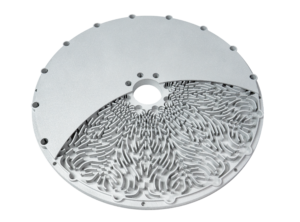
Metal additive manufacturing allows for the design and manufacturing of highly optimized components. When applied to semiconductor lithography and wafer processing equipment, complex metal AM parts like manifolds, wafer tables, wafer handling systems, flexures, and brackets improve performance and reliability of the part. These improvements enable system accuracy advancements at the nanometer level, and improved speed and throughput that ultimately results in more wafers processed and improved total cost of ownership. After working with AIG and building demand for complex AM parts among its customers, Wilting selected 3D Systems’ DMP Flex 350 for high quality in-house metal printing. For Wilting the new engineering collaboration with AIG will result in 1) reduced inertia and system vibration with up to 50% lighter parts for increased machine speed and up-time, resulting in more wafers processed, 2) 90% reduction in flow induced disturbance forces reducing system vibration and 3) realizing a 1-2 nanometer accuracy improvement, and improved reliability and design flexibility.
The AIG has also worked with high performance automotive companies to perform DfAM and AM process technology transfer on key assemblies and parts. In many of these instances the design focus is reducing mass while still maintaining function. This may mean working with elaborate materials such as titanium, or designing for thin-walled solutions. Historically, neither of these paths are particularly successful on the grand scale. In one such case with both of these requirements, AIG worked with a company to get a new gearbox designed and first production part printed using titanium. Benefits realized by engaging AIG for this effort were a smaller footprint for the first of its kind titanium gearbox, 2mm thick case walls, and a total gearbox weight (including steel internals) of under 150 lbs. Again, by leveraging AIG, the customer was able to not just create an AM line for production, but also was able to drastically modify the design to fit the overall targets for mass and to maintain performance requirements.
The Application Innovation Group isn’t just focused on high performance cars and semiconductor equipment – it is chartered with bringing additive manufacturing benefits to any advanced manufacturing process that requires tight tolerances, repeatable production with sub micron precision, and advanced materials. Additive Manufacturing generates large benefits in a market-of-one setting, as specific requirements that are tailored to exacting needs can be met – a great example is the dimensions required for a hip joint replacement for a specific individual, or a specific set of requirements which need to scale, like building a custom aircraft engine nacelle for a fleet (incidentally, according to ReportLinker, the aircraft nacelle and thrust reverser market is expected to reach $3.57 billion in 2026 at a compound annual growth rate (CAGR) of 7.73%), or even supporting spaceships and satellites (the AIG is currently involved in a program to operationalize RF components for an orbiting European satellite system). Repeatability, scalability, precision manufacturing, and digital definition are attainable with this technology – and those benefits are being realized through the skills of 3D Systems Application Innovation Group.


