


AI Technology, Inc. (AIT) Introduces Temporary Bonding Adhesives for Thin Wafer Handling
What do you use to handle thin wafers and thin reconstituted wafers? Increasingly miniaturized electronic devices require decreased profile heights, reduced foot-prints and ultimately, the perpetual thinning of wafers. Initially, working with thin wafers typically required temporary bonding of the wafer to a carrier and use of a temporary coating layer for wafer protection.
 For fan-out wafer-level packaging and 3D packaging, thin wafer handling is critical; the wafer must not warp, bend or shift during any wafer-processing steps. These wafer processing steps may involve different temperature ranges and exposure to a variety of chemicals depending on the processing steps such as etching, metallization, CMP, PVD, RDL in embedded, fan-out, and 3D wafer-level packaging.
AI Technology, Inc. (AIT) manufactures a series of temporary bonding materials for processing temperatures up to 150 Cº. They are well accepted for grinding, dicing, etching, and deposition. AIT customers prefer AIT bonding materials over conventional wax materials specifically because AIT’s products feature ease of use and quick removal, especially for very delicate compound wafers and photonics.
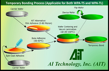
For higher temperature processing, AI Technology, Inc. (AIT) developed high temperature wafer processing adhesives (WPA) that can withstand processing temperature up to 330ºC. Also important is the chemical resistance of these WPA materials to acids and bases during the etching processes. The thermal and chemical stability allows these adhesive to maintain its chemical integrity allowing the thin wafer be separated from the wafer handler/carrier by heat-sliding or by laser de-bonding equipment. The WPA adhesive layer is designed to absorb UV breaking chemical bonds at the interface allowing for ease of separation. After separation, the WPA adhesive layer can be removed by peeling with minimum stress or solvent cleaning.
Besides supplying these WPA products in spin coating liquid, AI Technology, Inc. (AIT) also provides WPA as a thin film. This unique and innovative WPA-film minimizes processing time and total waste produced compared to a typical spin-coating process allowing higher through-put. In high volume manufacturing, some fan-out packaging involves reconstituted panels with larger dimensions compared to the traditional circular and small wafer size. For these high volume manufacturing panels, adhesive film in sheet format may provide the most efficient productivity. Typically heat-laminated onto a wafer first and followed by vacuum lamination of the wafer onto the carrier, AIT’s WPA thin film processing conditions and debonding techniques resemble the spin coating process used in WPA products.
AI Technology, Inc. (AIT) understands that different types of wafers, Si, GaAs, GaN, InP, glass, and sapphire are used in different applications and, depending on wafer processing conditions, demand highly specialized tools and equipment.
About AIT
Since pioneering the use of flexible epoxy technology for microelectronic packaging in 1985, AI Technology has been one of the leading forces in development and patented applications of advanced materials and adhesive solutions for electronic interconnection and packaging. AI Technology now has one of the highest reliability adhesives and underfills for die bonding for the largest dies, stack-chip packaging with dicing die-attach film (DDAF), flip-chip bonding and underfilling and high temperature die bonding for single and multiple-chip modules for applications beyond 230°C. The company continues to provide the adhesive solution for component and substrate bonding for both military and commercial applications. Its thermal interface material solutions of patented phase-change thermal pads, thermal greases and gels and thermal adhesives set many bench marks of performance and reliability for power semiconductors, modules, computers and communication electronics.
The company has an ISO9001:2008 certified manufacturing and R&D facility in the U.S. and a Far East Service Center in Hong Kong. The US headquarters has more than 50,000 square feet of manufacturing facilities for its die and substrate attached adhesive films and pastes, thermal interface materials (TIM) including insulated metal substrates, gap-filling compressible phase-change pads, thermal gels, thermal greases and adhesive films and pastes. AI Technology provides electromagnetic and radio frequency interference (EMI/RFI) mitigation material solutions including conductive gaskets, form-in-place (FIP) conductive gaskets, self-attached shielding covers/cans/lids, conductive caulks and adhesives, ultra-high temperature (300°C) continuous use films and paste die and component adhesives and advanced organic copper-clad laminates from 1/4 oz to 1 oz copper within its 16-acre campus in Princeton Junction, NJ.
AIT is committed to working closely with our customers and equipment suppliers to satisfy customer needs.
For more information, please visit www.aitechnology.com.


